Copyright © Chengdu Mini-Microwave Technology Co., Ltd. All Rights Reserved. Site Map
- +86-18180953121+86-15008407113
- 277434684@qq.com
- No. 68, Haichang Road, Huayang Street, Tianfu New District, Chengdu


1.Product composition and function
The frequency synthesize assembly consists of a pow supply and control circuit, a clock and local oscillator circuit, a receiving I local oscillator circuit, a receiving II local oscillator circuit, a transmitting local oscillator circuit,The circuit and the transmitting frequency conversion circuit are composed of six parts.
a)Clock and local oscillator circuit
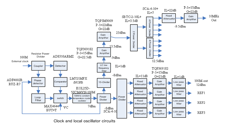
The clock and local oscillator circuit mainly consists of a coupler, a detector, a comparator, a phase detector, a loop filter, a DC switch, a divide-by-10 frequency divider, a 100M constant temperature crystal oscillator, power divider, low-pass filter, gain amplifier and other circuits.
The coupler, the detector and the comparator can monitor the input power of the external clock in real time, when the input power of the external clock is large enough.The external clock is synchronized with the internal clock by switching the DC switch.
The phase detector, the loop filter, the 10 frequency divider, the power divider and the 100m constant temperature crystal oscillator form a phase-locked loop,Can synchronize its output 100 MHz signal with that input 100 MHz reference clock.
A 10 MHz signal can be obtain after that output of the 100m constant temperature crystal oscillator passe through the power divider and the frequency divider by 10,After passing through a low-pass filter, a gain amplifier and a clock distributor, eight 10MHz clock signals can be obtained.
The output of the 100m constant temperature crystal oscillator passes through the power divider,A fixed attenuator, a gain amplifier and a low-pass filter output one channel of 100m synchronous clock signals and three channels of reference clock signals.
b)Power supply and digital circuit
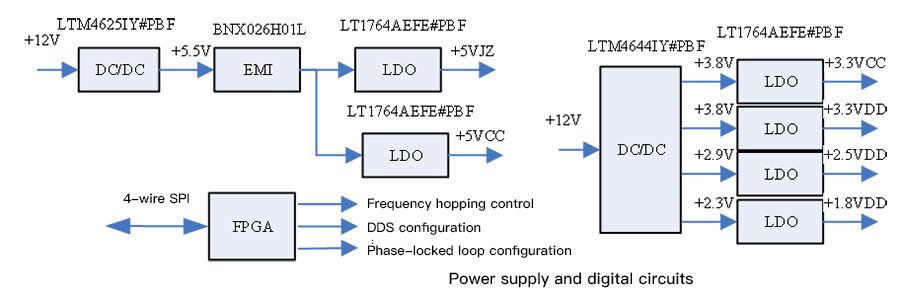
The power supply and digital circuit are mainly composed of FPGA chip, EMI filter, DC/DC power supply module, linear regulated power supply and other circuits.
EMI filter can effectively filter the power supply noise.The DC/DC power supply module and the linear regulated power supply are used for realizing voltage conversion and supplying power for internal active devices.The FPGA communicates with the host computer through a 4-wire SPI interface, which can realize the high-speed frequency hopping control of the output frequency.
c)Receiving 1 local oscillator circuit
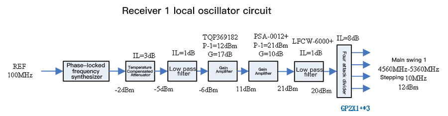
The receiving I local oscillation circuit mainly comprises a phase-locked frequency synthesizer, a gain amplifier, a temperature compensation attenuator, a fixed attenuator, a low-pass filter,Power divider and other circuits. The phase-locked frequency synthesizer is used for the parameter local oscillator signal.The gain amplifier is used to amplify the signal amplitude to meet the use requirements.The temperature compensation attenuator can compensate the temperature drift of the channel gain and keep the output signal power stable in the whole working temperature range.The fixed attenuator can adjust the channel gain. The low-pass filter is used to filter out the local oscillator harmonics.The power divider can divide one channel of local oscillator signal into four channels for output.
d)Receiving 1 local oscillator circuit
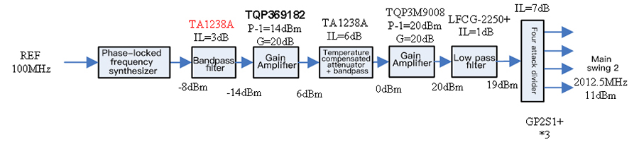
The receiving II local oscillation circuit mainly comprises a phase-locked frequency synthesizer, a band-pass filter, a temperature compensation attenuator, a gain amplifier, a low-pass filter,Power divider and other circuits. The 201.36 MHz bandpass filter is used to filter out out-of-band clutter and harmonics.The gain amplifier is used to amplify the signal amplitude to meet the use requirements.The temperature compensation attenuator can compensate the temperature drift of the channel gain and keep the output signal power stable in the whole working temperature range.The low-pass filter is used to filter out the local oscillator harmonics. The power divider can divide one channel of local oscillator signal into four channels for output.
e)Transmit local oscillator circuit
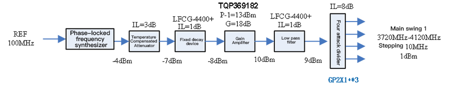
The transmitting local oscillator circuit is mainly composed of a phase-locked frequency synthesizer, a gain amplifier, a temperature compensation attenuator, a fixed attenuator, a low-pass filter,Divider and other circuits. The phase-locked frequency synthesizer is used for generating a local oscillator signal.The gain amplifier is used to amplify the signal amplitude to meet the use requirements.The temperature compensation attenuator can compensate the temperature drift of the channel gain and keep the output signal power stable in the whole working temperature range.The fixed attenuator can adjust the channel gain. The low-pass filter is used to filter out the local oscillator harmonics.The power divider can divide one channel of local oscillator signal into four channels.
f)Transmitting frequency conversion circuit
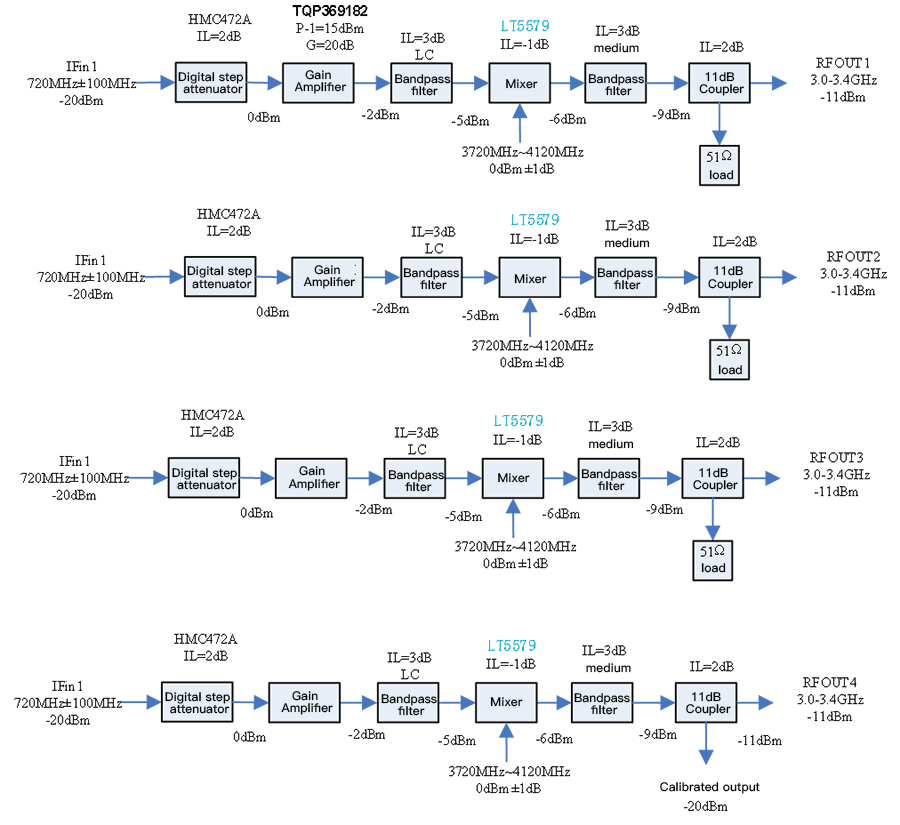
The transmitting frequency conversion circuit has four same channels,Each channel has a gain amplifier, a digital step attenuator, an if bandpass filter, a mixer, an RF bandpass filter, a coupler,Composition.
The gain amplifier can provide large enough power gain for the frequency conversion channel,The gain adjust function of that digital step attenuator enables the frequency convert to adjust the gain of the frequency converter under the condition of different input powerKeep the output power stable.
The intermediate frequency band-pass filter is used to filter the out-of-band noise of the input intermediate frequency signal.
The RF bandpass filter is used to filter out the mixing noise.
The mixer can mix 720MHz IF signal with 3720 ~ 4120MHz LO signal to obtain 3.0-3.4GHz RF signal.
A couple may couple a portion of that output radio frequency signal as a calibration signal output by the receiver.
2.Main functional indicators
1)8 channels of 10 MHz clock signals are generated.
2)4 channels of receiving I local oscillator signals are generated.
3)4 channels of receiving II local oscillator signals are generated.
4)Nerating four paths of transmission local oscillation signals.
5)One channel of 100M synchronous clock output signal is generated.
6)Receiving I local oscillator signal and transmitting local oscillator signal have frequency hopping function.
7)Up-converting the four paths of transmitting intermediate frequency signals into radio-frequency signals for output.
8)Coupling and outputting one channel of receiver calibration signal.
9)And can be automatically synchronize with an externally input 100MHz clock signal.
3.Main performance indicators
3.1.Receive local oscillator I
1)Output frequency: 4562.5MHz ~ 5350MHz.
2)Frequency hopping step: 12.5MHz.
3)Power: ≥ 10 dBm.
4)Spurious: ≤ -65dBc.
5)Phase noise ≤ -100dBc/Hz @ 1kHz.
6)Frequency conversion time ≤ 300 us.
7)Number of output channels: 4.
3.2.Receive II local oscillator
1)Frequency: 2012.5MHz.
2)Power ≥ 10 dBm.
3)Phase noise -100dBc/Hz @ 1kHz.
4)Spurious ≤ -65 dBc.
5)Number of output channels: 4.
3.3.Transmit local oscillator
1)Frequency 3725MHz ~ 4112.5MHz.
2)Frequency hopping step: 12.5MHz.
3)Power: 0 ± 1 dBm.
4)Spurious ≤ -65 dBc.
5)Step ≤ 10 MHz.
6)Phase noise ≤ -100dBc/Hz @ 1kHz.
7)Frequency conversion time ≤ 300 us.
3.4.Sample Clock
1)Frequency 10MHz
2)Power: 5 ± 2dBm
3)Phase noise: ≤ -130dBc/Hz @ 1kHz
4)Stray ≤ -80dBc
5)Number of output channels ≥ 8
3.5.Transmit input
1)Frequency: 720MHz ± 100MHz
2)Power: -20 ~ 10 dBm.
3)Number of input channels: 4
3.6.Transmit output
1)Frequency: 3000MHz ~ 3400MHz
2)Power: -11 dBm (need to adjust channel gain according to input power)
3)Output channels: 4 channels
4)Output clutter: ≥ 60dBc
3.7.Calibration output
1)Frequency: 3000MHz ~ 3400MHz
2)Power: -20 dBm ~ -25 dBm.
3)Output channel: 1
4)Output clutter: ≥ 60dBc
3.8.Sync Clock Output
1)Frequency: 100MHz.
2)Power: 10 ± 2dBm.
3)Number of output channels: 1.
4)Output clutter: ≥ 70dBc.
5)Output harmonic: ≥ 30dBc.
6)Phase noise: ≤ -155dBc/Hz @ 1KHz
7)Frequency stability: ≤ ± 0.1 ppm (guaranteed by design).
3.9.Sync Clock Input
1)Frequency: 100MHz.
2)Power: 3dBm ~ 13dBm.
3)Clutter: ≥ 70 dBc.
4)Harmonic: ≥ 30dBc.
5)Phase noise: ≤ -155dBc/Hz @ 1KHz (guaranteed by design)
6)Frequency stability: ≤ ± 0.1 ppm.
3.10.General indicators
1)Working temperature: -40 ℃ ~ + 60 ℃.
2)Power supply: 12 V/≤ 3.5A.
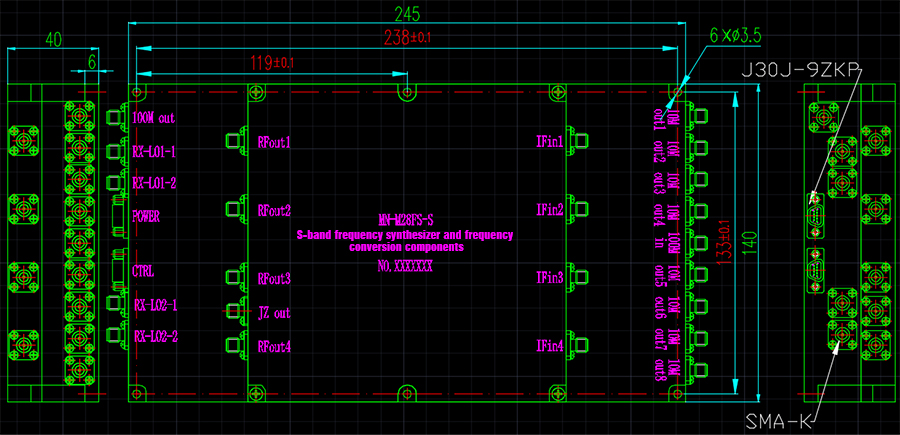
4.Interface and form factor
1)Receiving I local oscillator, receiving II local oscillator input, reference clock input, synchronous clock output, sampling clock output, transmitting input, transmittingOutput and calibration output interface: SMA-50K.
2)Power interface: J30J-9ZKP, see the table below for pin definition.
Pin number | Pin designator | Pin function | Remark |
1 | +12V | Power source |
|
2 | +12V | Power source |
|
3 | NC | Hanging in the air |
|
4 | GND | Power ground |
|
5 | GND | Power ground |
|
6 | +12V | Power source |
|
7 | +12V | Power source |
|
8 | GND | Power ground |
|
9 | GND | Power ground |
3)Power supply and control interface: J30J-15ZKP, see the table below for pin definition.
Pin number | Pin designator | Pin function | Remark |
1 | SS | Film selection |
|
2 | SCK | Clock |
|
3 | MISO | Master Input Slave Output |
|
4 | MOSI | Master Output Slave Input |
|
5 | DGND | Digitally |
|
6 | NC | Hanging in the air |
|
7 | NC | Hanging in the air |
|
8 | NC | Hanging in the air |
|
9 | NC |
|
|
10 | TDI | Program programming port |
|
11 | TDO |
| |
12 | TCK |
| |
13 | TMS |
| |
14 | DGND |
| |
15 | +3.3V |
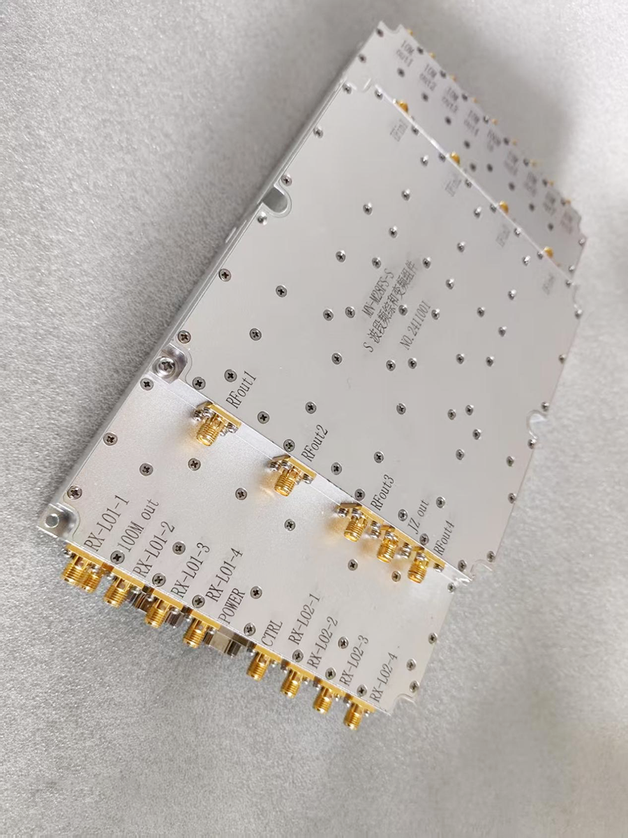
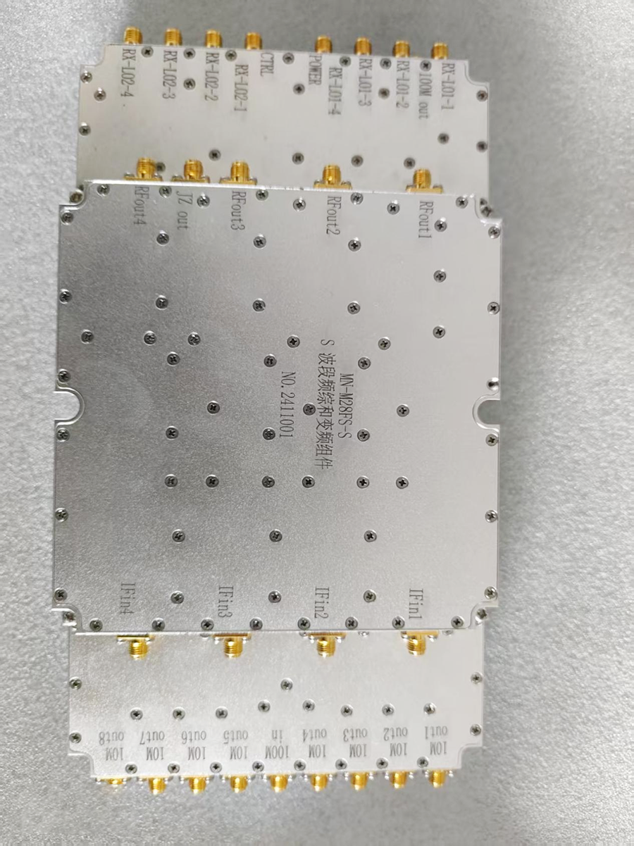
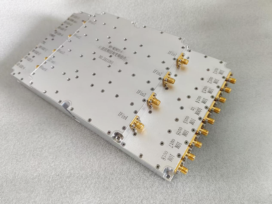
4)Dimension: 245mm * 140mm * 40mm.
5.Physical photos