Copyright © Chengdu Mini-Microwave Technology Co., Ltd. All Rights Reserved. Site Map
- +86-18180953121+86-15008407113
- 277434684@qq.com
- No. 68, Haichang Road, Huayang Street, Tianfu New District, Chengdu


1.Product composition and function
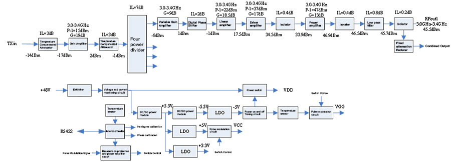
Fig. 1 Block Diagram of Product Circuit
As shown in the figure above,The power amplifier module is mainly composed of a temperature compensation attenuator, a gain amplifier, a power divider, a variable gain amplifier, a numerical control phase shifter, a linear amplifier, a drive amplifier, a power amplifier, an isolator, a low-pass filter, a coupler, a fixed attenuator, a single chip, an EMI filter,Voltage/current monitoring, DC/DC power supply, linear regulated power supply (LDO), power-on and power-off timing circuit, pulse modulation circuit, temperature detection andAn over-temperature protection circuit, a pulse protection circuit, a pow amplifier enable circuit and that like.
The RF variable gain amplifier is used to compensate the channel gain and ensure the output amplitude consistency of the four channels.
The phase shifter is used to adjust the channel phase to ensure the phase consistency of the four channels, and phase scanning can also be realized.
The output low-pass filter is used to filter the harmonics of the power amplifier.
The gain amplify, that linear amplifier, the drive amplifier and the power amplifier are amplify in cascade,A sufficiently large power gain of the module can be ensured.
The temperature compensation attenuator can compensate the temperature drift of the channel gain to ensure that the channel gain remains stable at full temperature.
The four-power divider can divide the power of one input signal into four outputs.
The isolator provides output reflection protection.
The coupler can realize output power coupling output and monitor the output power of the power amplifier in real time.
A fixed attenuator is used to adjust the coupled output power.
The product is powered by + 48 V, and the EMI filter can effectively filter the power supply noise.
The voltage and current monitoring circuit can monitor the working voltage and current in real time.
The temperature sensor can monitor the working temperature of the module in real time, and the over-temperature protection can be realized by cooperating with the power amplifier enabling circuit.
The negative voltage protection of GaN power amplifier can be realized by the combination of power-on and power-off sequential circuit and 48 V power switch.
The pulse width protection circuit can automatically detect the modulation pulse width of the power supply, and automatically turn off the power amplifier when the pulse width exceeds the standard, so as to prevent the power amplifier from being burnt.
The power amplifier enable circuit can realize the independent switch control of four power amplifiers through software, which is convenient for debugging and testing.
The DC/DC power supply and LDO provide voltage conversion to power the internal active circuitry.
And that pulse modulation circuit can realize the pulse modulation of the pow supply of the power amplify.
The grid voltage temperature compensation circuit of that pow amplifier can realize the temperature compensation of the output pow of the power amplifier,And that output pow of the power amplify is kept stable under the full temperature line.
2.Main functional indicators
1)Power distribution and 4-channel power amplification.
2)And has a coupling output function.
3)Power supply pulse modulation function.
4)The 4-channel power amplifier has an independent switch enable function.
5)The 4-channel power amplifier has independent phase adjustment function.
6)Monitoring of working voltage, current and working temperature.
7)Channel gain adjustment function.
8)It has the functions of working parameter configuration and working status query.
9)With over-temperature protection, negative pressure protection, output mismatch protection functions.
10)Continuous wave operation is supported under small signal.
11)It has the function of preventing rain.
2.Main performance indicators
1)Number of RF input ports: 1
2)RF input frequency: 3.0 GHz ~ 3.4GHz
3)RF input power: -14 dBm.
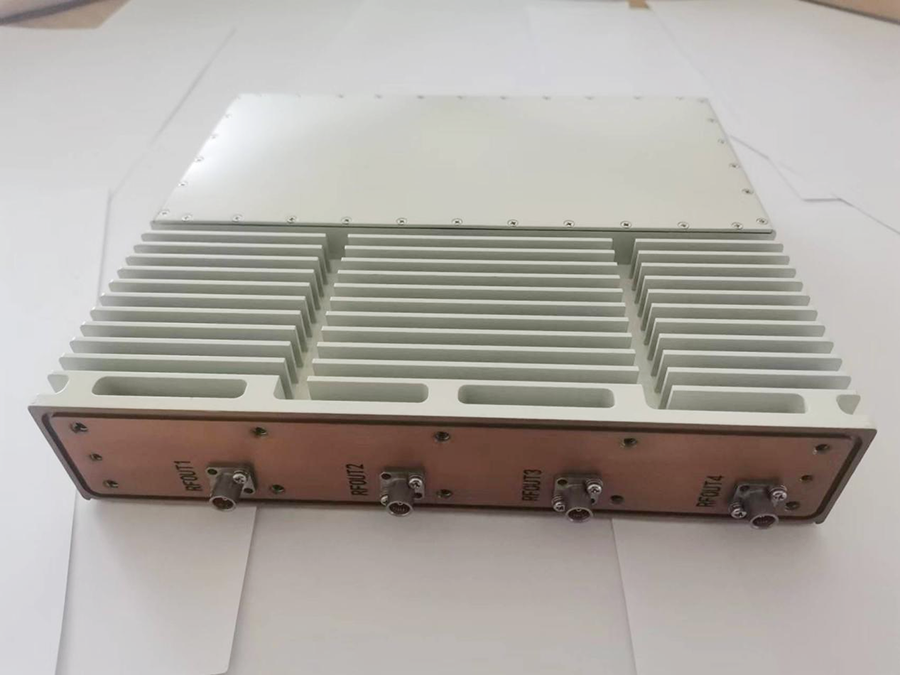
4)Number of RF output ports: 4
5)RF output frequency range: 3.0GHz ~ 3.4GHz.
6)RF output power: ≥ 45dBm.
7)Attenuation adjustment range: ≥ 30 dB.
8)Attenuation adjustment step: 0.5dB.
9)Phase adjustment range: 0 ~ 360 °
10)Phase adjustment step: 5.625 °
11)Coupling output power: 5dBm ± 3dB.
12)Pulse width: ≤ 200uS.
13)Duty cycle: ≤ 20%.
14)Output harmonic power: ≤ -30 dBm.
15)Top drop of pulse signal: ≤ 0.5dB.
16)Pulse signal rising and falling edge: ≤ 100ns.
17)Pulse modulation delay: ≤ 1uS.
18)Input and output standing wave: ≤ 2.
19)Amplitude consistency between channels (realized by software compensation): ≤ ± 0.5dB.
20)Inter-channel phase consistency (realized by software compensation): ≤ ± 5 °.
21)Clutter suppression (small signal continuous wave test): ≥ 60dBc.
22)Intrapulse clutter: ≥ 80dBc.
23)Working temperature: -40 ℃ ~ + 60 ℃.
24)Power supply: 48 V/≤ 3 A.
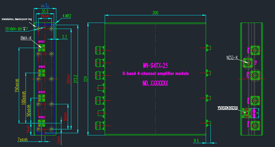
3.Interface and form factor requirements
1)RF input and coupling output interface: N (S) -50K.
2)RF output interface: BMA-50K
3)Power and control interface: Y50EX0810ZJ10, see the table below for pin definition.
Pin number | Pin designator | Pin function | Remark |
1 | TXD+ | RS422 interface | Used to configure the operating frequency, channel attenuation, and operating mode. Query operating status: operating frequency, attenuation configuration, operating mode, operating voltage, operating current, operating temperature, lo lock status |
2 | TXD- | ||
3 | RXD+ | ||
4 | RXD- | ||
5 | PTT | Switch control | High level power amplifier on, low level power amplifier off |
6 | DGND | Digitally |
|
7 | +48V | Power source |
|
8 | +48V | Power source |
|
9 | GND | Power ground |
|
10 | GND | Power ground |
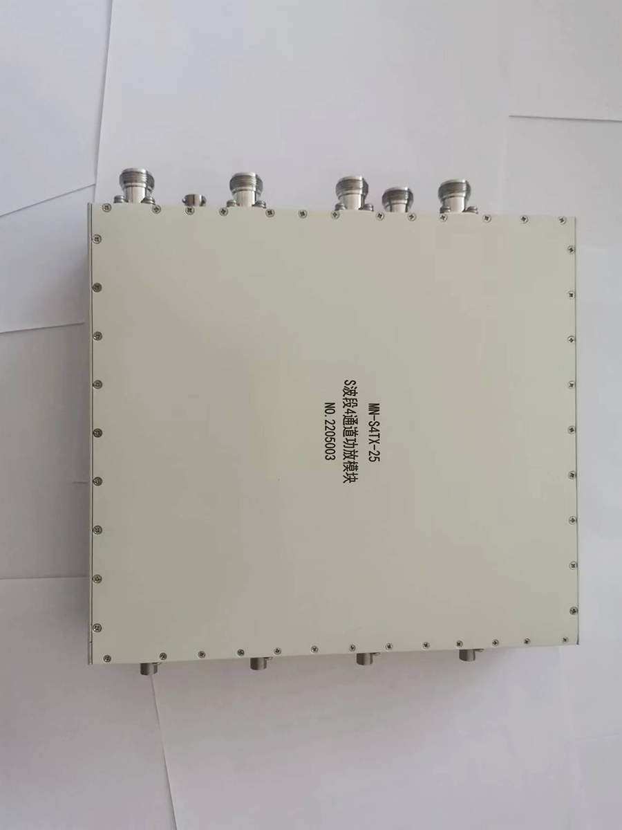
4)Dimension: 200mm * 224mm * 44mm.
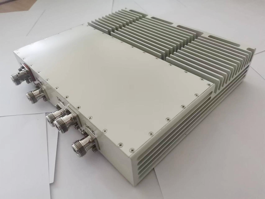
4.Physical photos of the product